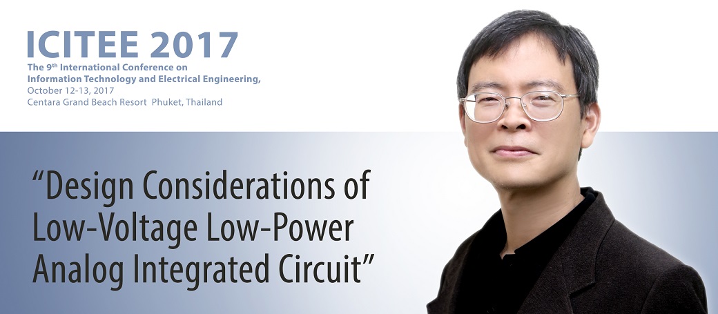
Varakorn Kasemsuwan
King Mongkut's Institute of Technology Ladkrabang
Abstract
In practice, every signal in the physical world is continuous with respect to time. Examples of analog signal sources are microphone, temperature sensor, humidity sensor, photo cells in digital camera and RF signals in space and at antenna. Analog circuit serves as a bridge to connect between the physical world and the powerful digital computing signal-processing systems. The power of digital signal and information processing can only be useful only if analog interfaces (e.g., anti-alias filter, reconstruction filter and analog-to-digital and digital-to-analog converters) with sufficient performance are available.
Several analog circuit designs have been transformed over the past decades. An integration of analog integrated circuits along with digital integrated circuits known as mixed signal integrated circuit has led to the use of smaller dimension devices. Integration cost and circuit size are the main driving force towards a full integration of the analog interfaces and digital signal processing on a single die. In addition, cost and circuit size considerations also push towards finer line widths.
It is known that the line width of CMOS technologies moves toward nanoscale dimensions. This will result in an increase of the functionality density, the intrinsic speed of the devices and thus the signal processing capability of the circuits. However, as the thickness of the gate oxide is reduced, the supply voltage needs to be proportionally reduced in order to prevent the transistor from breakdown due to higher electrical field across the gate oxide, and to ensure its reliability. In addition, recent advances in the implantable biomedical sensor system that could be worn by people, monitor physiological parameters, and even provide some kind of treatment is progressing very aggressively. Obviously, the proliferation of this type of remote control and other mobile communication equipment mandate the development of low voltage and low power analog integrated circuits.
Conventional analog circuit design techniques are basically well suited mostly for high power supply voltages, where transistors can be stacked, and still there is enough voltage headroom for signal swings. Unfortunately, the finer line widths of CMOS technologies is mostly beneficial to digital integrated circuit, however, lead to several analog performance degradations. This degradation mainly comes from the fact that the threshold voltage (VT) and saturation voltage (VDSAT) of MOSFET are still relatively high for the given supply voltage range. As a result, analog circuit suffers from reduced input and output signal swings, reduced small-signal output resistance and intrinsic gain and increased input referred noise.
There has been a strong interest in developing analog and mixed-signal design techniques that deal with these challenges. These include bulk-driven MOSFET, floating-gate MOSFET, common-mode level shifting, subthreshold operation, self-cascoded MOSFET and switched op-amp. Each technique will be presented and discussed. Advantage and disadvantages of individual technique will be addressed. Finally, a guideline to choosing appropriate circuit technique will be explained and summarized.
Biography
Dr. Varakorn Kasemsuwan received the Bachelor degree from King Mongkut’s Institute of Technology Ladkrabang (KMIT) Thailand in 1989, the M.S. and Ph.D. degrees from University of Pittsburgh, in 1993 and 1997, respectively. At present, he is working as a lecturer at KMITL. His research interests include semiconductor device modeling and analog integrated circuit design focusing on low voltage and low power applications.